 |
|
NANOTECHNOLOGY UNDERGRADUATE EDUCATION - 2007 In Situ Real-time Atomic Scale Nanostructural Synthesis, Characterization and Modeling |
|

Click on Image to View Movie
Alongside is a movie of Germanium quantum dots growing on the (100) surface of silicon at above 500oC in a very low pressure germane environment. The images have been numerically differentiated to clearly show the {105} facets on the dots. The model below clearly shows facets and enables calculation of the number of atoms in the dot and other growth parameters.
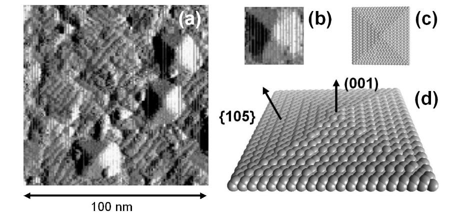
Fig. (a) Differential SPM image extracted from a real-time growth sequence showing a number of pyramidal islands growing in close proximity to one another (b) magnified view of a 28 nm (edge dimension) island (c) 3406-atom model (edge length ~17 nm) viewed from above, (d) magnified view of the atomic scale model illustrating the structure of the various crystalline facets involved.
Click on Image to View Movie
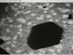
In situ growth of Cu-Cr and Cu-Ti alloys in low pressure ammonia at about 600oC. Here, the growth of faceted copper nanocrystals is seen. The parallel facets are {100} and the inclined facets are {111}. Growth proceeds in "bursts" on individual facets and is not continuous. This crystal is viewed along <110>. Note that no {220} facets are present. Why not? What are the relative surface energies of {111} and {100} nanofacets?
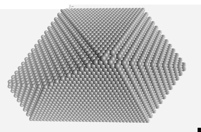
Fig. The model aboveshows the atom arrangements on the surface nanofacets
Click on Image to View Movie
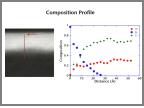
An annular dark field STEM image is shown on the left. The vertical red line shows the path for nanochemical analysis. Silicon is at the bottom (dark) and crystalline hafnium oxide (light) at the top, 40 Angstroms thick. These two are separated by a 10 Angstrom thick layer of silicon monoxide. As the probe moves up the red line the compositions of hafnium, silicon and oxygen are plotted out on the right side graph. Silicon extends halfway through the hafnium oxide layer, and hafnium extends into the silicon monoxide layer. We see that these nanolayers do not have atomically sharp chemical interfaces, which has a large effect on their properties. These analyses were done with an electron probe of 2.5 Angstrom diameter, i.e., about 2 atoms in diameter. A plot of the probe current distribution is shown at left. The Gaussian function fitted to the smooth experimental probe shows that students can easily learn to model it quite accurately.
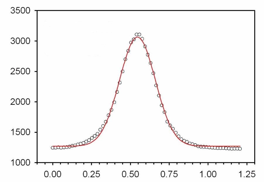
Fig. Circles are experimental probe current distribution; FWHM=0.25 nm. Red: Gaussian model
Click on Image to View Movie
Carbon nanotubes are synthesized by a "chemical vapor deposition" process in which a metal nanoparticle catalyses the nucleation and growth of these nanotubes in the presence of a gaseous hydrocarbon precursor under suitable reaction conditions. Recent developments in Transmission Electron Microscopy instrumentation have made it possible to make in-situ observations of gas-solid interactions (here, hydrocarbon precursor - metal nanoparticle/ carbon nanotube interaction) at the atomic scale using an Environmental Transmission Electron Microscope (ETEM).
The included video footage is a series of images showing direct observation of growth of carbon nanotubes.
In this experiment, Nickel nanoparticles were preheated to a temperature of about 500ºC followed by subsequent introduction of around 20 mTorr of acetylene (Molecular Formula: C2H2) into the reaction chamber. A simplified description of growth mechanism involves a process in which the carbon atoms, decomposed from acetylene onto the metal nanoparticles, get absorbed into the nanoparticle to form a carbon-nickel solid state solution. As supersaturation occurs the carbon atoms migrate from the nickel catalyst particle to the end of the nanotube in contact with the nickel particles, leading to the growth of nanotube. The nickel nanoparticles remain anchored to the end of the nanotube during the growth process.
| The LeRoy Eyring Center for Solid State Science PO Box 879506 Engineering Center G Wing, Room 307 Tempe, AZ 85287-9506 Office Phone: (480) 965-4544 Fax: (480) 965-9004 |
|
| Contact Webmaster |