
Around 1980 a new revolutionary method of microscopy known as scanning probe microscopy (SPM) was invented and in a scant ten years, the applications have been increasing exponentially in fields as diverse as surface physics, chemistry, geology, biology and optics. SPM is also beginning to emerge as a useful and popular technique for R&D, quality control in several industries such as the semiconductor and big-technology industries. tremendous potential of the SPMs- a relatively inexpensive, easy to operate table-top family of instruments in innovations in undergraduate science and engineering education. Our objective is simple - to exploit the incredible potential in teaching students about fundamental concepts, integrate learning across traditionally seperated disciplines, while at the same time conveying to them the excitement at the forefront of scientific research. The hands-on approach, the high visual impact, the interactive computer interface, ability to learn about surfaces, their properties and even manipulate them at the atomic level, immediately captures and maintains the student's interest. The beauty of this technique is that it naturally cuts across boundaries of traditional disciplines such as natural sciences, engineering and mathematics and hence can be a powerful catalyst for integration in education. It can go a long way in training future generation of students who can work with and understand fields other than their specialization, in order to solve complicated technological problems through effective collaborations.
All probe microscopes have two features common features : a) a sharp, tiny probe gets very close to the sample and feels the surface by monitoring some kind of interaction, between the probe and the surface, which is very sensitive to distance. B) the sample or the probe is scanned in a rastor fashion with near atomic accuracy and the variation in the interaction is translated to a topographic map of the surface.
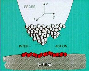
Among the family of SPM's the two most commonly used are Scanning Tunneling Microscopy (STM) and Atomic Force Microscopy (AFM). In STM, a sharp metallic probe and a conducting sample are brought together until their electronic wave functions overlap. By applying a potential bias between them, a tunneling current is produced. The probe is mounted on a piezoelectric drive that scans the surface. Combining the piezoelectric drive with a feedback loop allows imaging of the surface in either a constant current or a constant-height mode. In AFM, the probe tip is attached to a cantilever with a small spring constant. The probe is much like a spring which changes dimension upon experiencing a force ( Hookes' law) and the interaction that will be monitored is the repulsion between two atoms when they are brought extremely close to each other. The forces acting on the probe tip deflect the cantilever and the tip displacement is proportional to the force between the surface and the tip. The resultant bending of the AFM cantilever is measured optically by the deflection of the reflected laser beam. The most important advantage that AFM has over STM is that the former is not limited to conducting samples, so materials can often be imaged "as is" with essentially no sample preparation.

Using the above state-of-the-art nobel-prize winning (in 1986 for physics) technology, you will image two very familiar samples - a) the Compact Disk (CD) that we all use nearly everyday to listen to music and b) Graphite - a crystalline form of carbon that is in lead pencils that we write with.
In the case of the CD you will be able to see the manner in which the musical information is stored. (the magnifications used will be of the order of 10,000). You will be able to compare this with the results on the cd obtained with the optical microscope and sem. You will also compare the surface features of the LP record using a profilometer. Fig.3 shows an AFM image of a CD stamper.
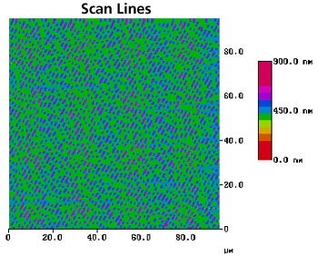
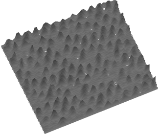
Figure 3. An atomic force microscope image of a CD stamper. The stamper has raised knobs that make tiny pits in the CD when it is stamped. These pits are scanned by the laser and the resulting digital signal is converted into an audio signal. The color coding above conveys the height of the knobs in nanometers (nm). The lower image is a 3-dimensional projection of a portion of the CD stamper.
Return to the Readings Page
Go Back to the Previous Page
Reading by B.L. Ramakrishna, Center for Solid State Science, Arizona State University
Page authored by the ACEPT W3 Group
Department of Physics and Astronomy, Arizona State University, Tempe, AZ 85287-1504
Copyright © 1995-2000 Arizona Board of Regents. All rights reserved.