Silicon -- a Material Transparent to InfraredThe semiconductor silicon (Si) is an element with 14 electrons surrounding the positively-charged nucleus. Silicon has the property that it is transparent to low energy in the infrared portion of the spectrum but it is opaque to photons in the visible portion of the spectrum. This transparency of silicon to the infrared (IR) is a property of the manner in which the atoms are bonded together; in this case, covalent bonds.Covalent bonding between two silicon atoms is visualized as a sharing of electrons supplied by both atoms. The bond comes about because shared electrons orbit around both atoms. This overlap of the bonding orbitals lowers the energy of the system. For the purpose of bonding, the atoms of silicon may be visualized as having 10 inner, closed-shell electrons (which do not participate in bonding), and four outer electrons that do. When a silicon atom is brought together with four other silicon atoms (Fig. 1), it shares its four outer electrons (heavy, curved lines in Fig. 1) with each of the four atoms. These atoms, in turn, share one of their four outer electrons (light, curved lines) wiht the central Si atom. Covalent bonds are quite directional (the four electrons are arranged symmetrically) as illustrated
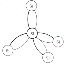
Figure 1. Covalent bonds of silicon by the tetrahedral configuration. Again, we emphasize that these lines are just a pictorial representation of a more diffuse electron distribution. Figure 2 is a two-dimensional representation of the silicon lattice. The covalent bonds are shown by the curved lines connecting the Si atoms. Although this is a line-and-ball representation, it shows that all the outer or valence electrons are tied up in covalent bonds. The inner 10 electrons are tightly bound (binding energies greater than 100 eV) and the outer four form the covalent bonds. Consequently, there are essentially no free electrons available for charge transport.
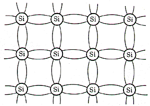
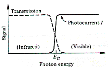
Figure 2. Two-dimensional representation of the Si lattice for high-purity Si, where all the outer electrons are in covalent bonds. If we shine light of a fixed energy on the sample, we can break the bonds if the photon energy is greater than the bond energy (about 1.1 eV for Si), which corresponds to the infrared portion of the spectrum. When a bond is broken, the liberated electron is now free to move within the crystal. The empty site, or hole, left by the escaping electron can be occupied by a nearby electron. Consequently, the hole can also migrate through the crystal by exchanges with the bound electrons. Both electrons and holes can trasnport charge leading to a current, a photocurrent. If the sample is irradiated with low-energy photons which are not energetic
enough to break the covalent bonds, the photons will be transmitted through
the sample unattenuated (Fig. 3). There is no mechanism for the absorption
of light as well as no photocurrent. As the energy of the photons is increased,
a threshold is reached where the interaction of light with the Si lattice
can break the covalent bonds. In Si this occurs at an energy EG
of about 1.1 eV, at a wavelength
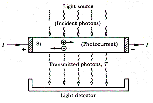
Figure 3. Photons incident on a silicon sample, with the lower portion displaying the signal from the transmitted photons (not absorbed) and the photocurrent versus photon energy. As the photon energy is increased above this energy EG, the number of transmitted photons decreases and the photocurrent increases due to the absorption of light in the bond-breaking process. Each method, transmission or photoconductance, can be used to measure the energy required to free and electron from the covalent bonds. We have presented the relatively simple case of Si. A compound semiconductor such as a III-V compound, gallium arsenide (GaAs), also forms a lattice with covalent bonding. The similarity to Si can be inferred from Fig. 4 which shows a portion of the periodic table and a representation of the atomic configuration of the electrons.
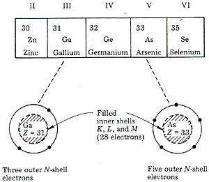
Figure 4. Portion of the periodic table and representation of the electron distribution around gallium (three outer electrons) and arsenic (five outer electrons). All five elements have 28 electrons in filled inner shells (K, L, andM shells) and electrons in the outer, less tightly bound shell (N shell). The column III element GA has three outer electrons, and the column V element As has five outer electrons. When these two elements are arranged in a lattice they share outer electrons to form covalent bonds with Ga atoms providing three electrons and As atoms, five electrons. There is, in effect, a Ga sublattice and an As sublattice (Fig.5).
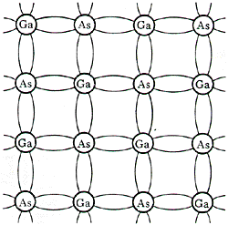
Figure 5. Two-dimensional representation of the gallium-arsenide (GaAs) lattice for high-purity GaAs, showing that all the outer electrons are in covalent bonds. The compound gallium arsenide has the same response to light that silicon does: transparent to infrared light which is unable to break the electron bonds and opaque to visible light which can break bonds. Almost all the paint pigments have the same properties as Si and gallium arsenide. They are transparent to infrared light. This transparency to IR occurs because the paint pigments are nearly all oxides (such as titanium white, titanium oxide) or sulfides (such as the red vermilion, mercury sulfide). In pure form, they are insulators or semiconductors with almost no electrons available for light absorption in the IR. Page authored by ACEPT W3 Group Department of Physics and Astronomy, Arizona State University, Tempe, AZ 85287-1504 Copyright © 1995-2000 Arizona Board of Regents. All rights reserved. |